亚洲精品无码Av人在线观看国产_精品制服日韩国产第一 色妞www精品视频二_日韩人妻无码AⅤ中文字幕你懂的

Mailbox verification
Your email:
Verification Code:
SLP74AUP1G74
LOW-POWER SINGLE POSITIVE-EDGE-TRIGGERED D-TYPE FLIP-FLOP WITH SET AND RESET

     The SLP74AUP1G74 provides solution to the industry's low-power needs in battery-powered portable applications. 

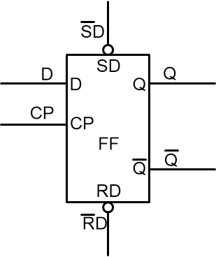
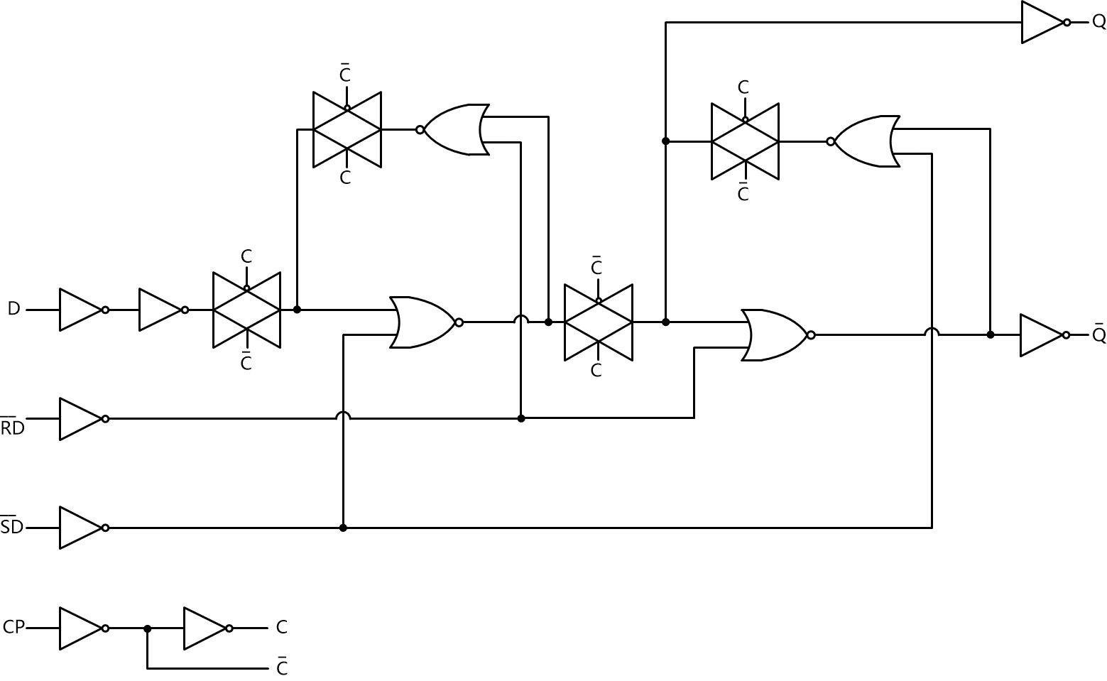
     It provides a low-power, low-voltage single positive-edge triggered D-type flip-flop with individual data (D), clock (CP), set (S__D) and reset (R_D) inputs and complementary Q and Q__ outputs. The S__D and R_D are asynchronous active LOW inputs and operate independently of the clock input. Information on the data input is transferred to the Q output on the LOW-to-HIGH transition of the clock pulse. The D input must be stable one set-up time prior to the LOW-to-HIGH clock transition for predictable operation. 

Schmitt trigger action at all inputs makes the circuit tolerant to slower input rise and fall times across the entire VCC range from 0.8V to 3.6V.

     This device ensures a very low static and dynamic power consumption across the entire VCC range from 0.8V to 3.6V, resulting in increased battery life. 

    This device is fully specified for partial power-down applications using IOFF. The IOFF circuitry disables the output, preventing the damaging backflow current through the device when it is powered down.

Main feature
  • Wide supply voltage range from 0.8V to 3.6V

  • Low static power consumption; ICC = 0.9μA (maximum)

  • Inputs accept voltages up to 3.6 V

  • Low noise overshoot and undershoot < 10 % of VCC

  • IOFF circuitry provides partial power-down mode operation

  • ESD protection:

  • HBM exceeds 5000 V

  • CDM exceeds 1000 V

  • Latch-up performance exceeds 100 mA

  • Specified from -40°C to +85°C and from -40 °C to +125 °C

Ordering Information
Product Name Package form Marking Hazardous Substance Control Packing Type Remarks
SLP74AUP1G74JWTR VSSOP-8-100-0.5 1G74 Halogen free Tape&Reel
Block Diagram

SLP74AUP1G74-圖1.png

Fig.1 Functional diagram


SLP74AUP1G74-圖2.png

Fig.2 Logic diagram for one flip-flop